VisualApplets Fundamentals#
Introduction and Purpose of This Document#
Key Terms
Throughout this tutorial, boxes labeled Key Terms explain common terms for readers who do not know them yet.
VisualApplets is the design tool on the PC. The FPGA is the chip on the frame grabber. You draw the pipeline in VisualApplets. The build configures that pipeline as hardware on the FPGA. Camera data is processed on the frame grabber, not in the VisualApplets editor.
Basic Design Concepts#
VisualApplets lets you create image-processing functionality on FPGA-based programmable hardware without writing code in a hardware description language like VHDL or Verilog. You build a design in a graphical way from library operators and connect them so that image data flows along defined paths.
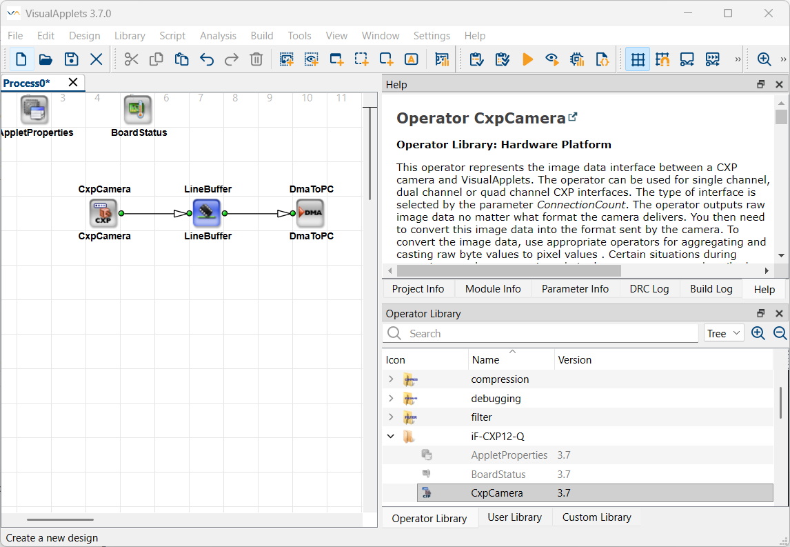
Additionally, you can create and edit designs using the Python and Tcl scripting languages.
On a programmable frame grabber, the camera or another image source delivers a continuous pixel stream into the acquisition path, and the FPGA on that board processes that stream. What you build is not a program the FPGA fetches and executes like a CPU. Instead, the build configures a dedicated digital circuit on the FPGA whose structure matches your pipeline.
You create and edit the VisualApplets design on the PC (operators, modules, and links in a *.vad file). The build step then translates that pipeline into hardware logic.

In such a VisualApplets design, you instantiate operators from the operator libraries; each instance of an operator in a design is called a module. Modules are connected by links, and the order of processing is determined by how you arrange and connect those modules. Together, the modules and links form an image-processing pipeline that defines how pixel data move through acquisition, processing, and output stages.
When this tutorial says that a module processes, buffers, blocks, or transfers data at runtime, it refers to the FPGA logic generated from that module. The graphical module in VisualApplets describes that hardware behavior; it does not itself process runtime camera data.
You save the editable design as a *.vad file. When you build the design for a specific target frame grabber, VisualApplets produces a binary hardware applet file with extension *.hap. You load this file onto the frame grabber. Don't treat the *.hap file as an editable design source. You always change the *.vad design and build again. At runtime, you can still change dynamic write parameters that your application or runtime tools write to the device.
The practical goal is real-time image processing in hardware. While you edit and validate the pipeline as a *.vad project on the PC, only the built *.hap carries that processing logic and data-flow structure onto the FPGA as runnable hardware.
Key Terms
Build means turning your graphical design in VisualApplets into a configuration that the frame grabber FPGA can run.
A hardware applet, with file extension *.hap, is that runnable result.
A frame grabber is an expansion board in the computer that receives the camera data, hosts the FPGA, and runs the applet you built. VisualApplets does not contain the FPGA.
FPGA Technology#
A field-programmable gate array (FPGA) is a chip that contains a large number of programmable logic elements. Those elements and the on-chip routing can be configured to realize complex digital circuits in hardware that perform many operations in parallel.
When you build a VisualApplets design for a target frame grabber, VisualApplets automatically maps your operators and links onto FPGA logic. You do not implement that mapping yourself. VisualApplets handles the vendor-specific FPGA toolchain (typically Xilinx Vivado) for placement, routing, and bitstream generation. See Basic Design Concepts for how the *.vad project on the PC relates to the *.hap that configures the FPGA.
Besides programmable logic elements, which you typically use to build combinational circuits, an FPGA provides flip-flops for clocked storage, block RAM for line buffers and other on-chip memory, and DSP or arithmetic slices for fast multiply‑add and similar functions. As part of the same automated build flow, VisualApplets maps operators and links onto these resources. Each operator in your design corresponds to concrete hardware such as logic, memory, arithmetic, or a mix.
The FPGA resources your design needs depend on how many modules you use, which operators you choose, and how you set parallelism, buffer sizes, and other parameters. Heavier use of logic, memory, or parallel data paths increases consumption. If the design exceeds what the device can implement, the build fails or you may not achieve timing closure. VisualApplets estimates and reports FPGA resource consumption when you run Design Rules Check Level 2 (DRC Level 2). See FPGA Resource Estimation in the User Manual and Design Rules Check in the User Manual. For further explanation of how consumption builds up, which rules apply, and how you trade off design choices, see also the Parallelism Tutorial topic and the Memory Elements Tutorial topic.
Pipeline Execution in Hardware#
On the frame grabber, the built hardware applet implements your design as a pipelined hardware path: pixel data move through linked module stages in a continuous flow.
The pipeline you draw in VisualApplets is a model of the hardware path on the FPGA: The FPGA handles data stage by stage and passes it downstream in a continuous flow. The design doesn't assume that the pipeline stores an entire image at every stage along the path. The generated FPGA pipeline transfers data from stage to stage on clock cycles according to this pipeline model, as described in more detail in the Pipeline Concept Tutorial topic.

Compared with a typical CPU workflow, which often moves large blocks of data through memory and executes instructions largely in sequence, an FPGA can process and transfer data pixelwise in parallel along the pipeline. Compared with a GPU, which runs many threads over data under program control, an FPGA pipeline is closer to a fixed conveyor. Data moves through processing stages that you wired in the design. This is why documentation uses the pipeline metaphor so often.
Key Terms
- Think of an FPGA as a chip on the frame grabber where many small operations run at the same time along a path you designed in VisualApplets. The build turns that design into dedicated hardware logic on the FPGA. Pixel data then flow through those hardware stages like items on a conveyor, which is the pipeline idea.
- A CPU usually works through steps one after another and frequently loads and stores whole chunks of data.
- A GPU runs the same kind of operation on many pixels or threads in parallel under a program.
Clock Cycles and Timing#
FPGA designs rely on a clock signal that tells each pipeline stage when to capture, transfer, and process data. VisualApplets and this tutorial call that clock the Base Design Clock. It is the clock of the generated FPGA pipeline. It is not the same as the camera pixel clock. A clock cycle is one tick of the Base Design Clock. On each rising clock edge, flip‑flops in the pipeline store their input data and pass it to the next stage.
Clock cycles therefore:
- Define the timing of all elements such as registers in the pipeline.
- Ensure stable data flow, because values only move to the next stage at predictable clock edges.
- Determine the maximum processing speed, since the Base Design Clock frequency must be slow enough for all combinational logic between registers to settle correctly before the next cycle.
In other words, the clock rhythm keeps the entire hardware pipeline aligned. Individual operators are pipelined as well: the build implements each operator with internal register stages so the FPGA stage can accept new input on every clock cycle, even when a single input needs several cycles before its result appears at the output. After the pipeline has filled, throughput at the output can still be one result per cycle while the latency from a given input to its result may be greater than one cycle. That is why pipelining and resource mapping during the build directly influence the achievable Base Design Clock frequency and throughput.
Info
You find the Base Design Clock frequency and other hardware resource information about your frame grabber in Device Resources.
Related Topics#
- From Empty Design to Running Applet Tutorial topic — design, DRC, simulation, and build
- Pipeline Concept Tutorial topic — how data moves through the pipeline
- Parallelism Tutorial topic — bandwidth, clock, and FPGA resources
- Memory Elements Tutorial topic — FPGA memory and frame grabber DRAM
- Device Resources — Base Design Clock and platform resources
- Design Rules Check in the User Manual — DRC Level 1 and Level 2