After you have finalized the implementation, it is recommended to perform a Design Rule Check Level 1 and 2. To perform a Design Rule Check Level 1 and 2, select Analysis+Design Rules Check Level 1 and 2 or use the icon from the icon bar.
Design Rule Check Level 1 reports formal errors in the implementation and their exact location in the design. You must correct these errors before the design can be translated to a hardware applet.
Design Rule Check Level 2 additionally gives information about the estimated FPGA resources used in the design. With this information you can check, whether enough FPGA resources are available for your image processing implementation. If the resources exceed 100% of one of the FPGA resources, you need to redesign your implementation to save resources.
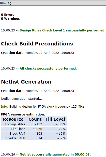
In Figure 175, 'Design Rule Check 1 and 2 for the Example Design
Sobel_Filter.va' the result of Design Rule Check 1 and 2 is
shown: Everything is designed correctly and about 36% of the available Lookup
Tables, 22% FlipFlops, 15 % Block RAM and 2 % of the available embedded ALUs are
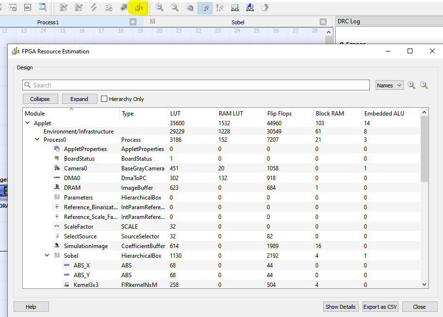
used. You can see a detailed overview on how many FPGA resources each element in
the design consumes (see Figure 176, 'FPGA Resource Estimation') under Analysis+FPGA Resource Estimation